A new video shared online today provides some interesting information on the Nintendo Switch 2, such as the process node used for the SOC and more
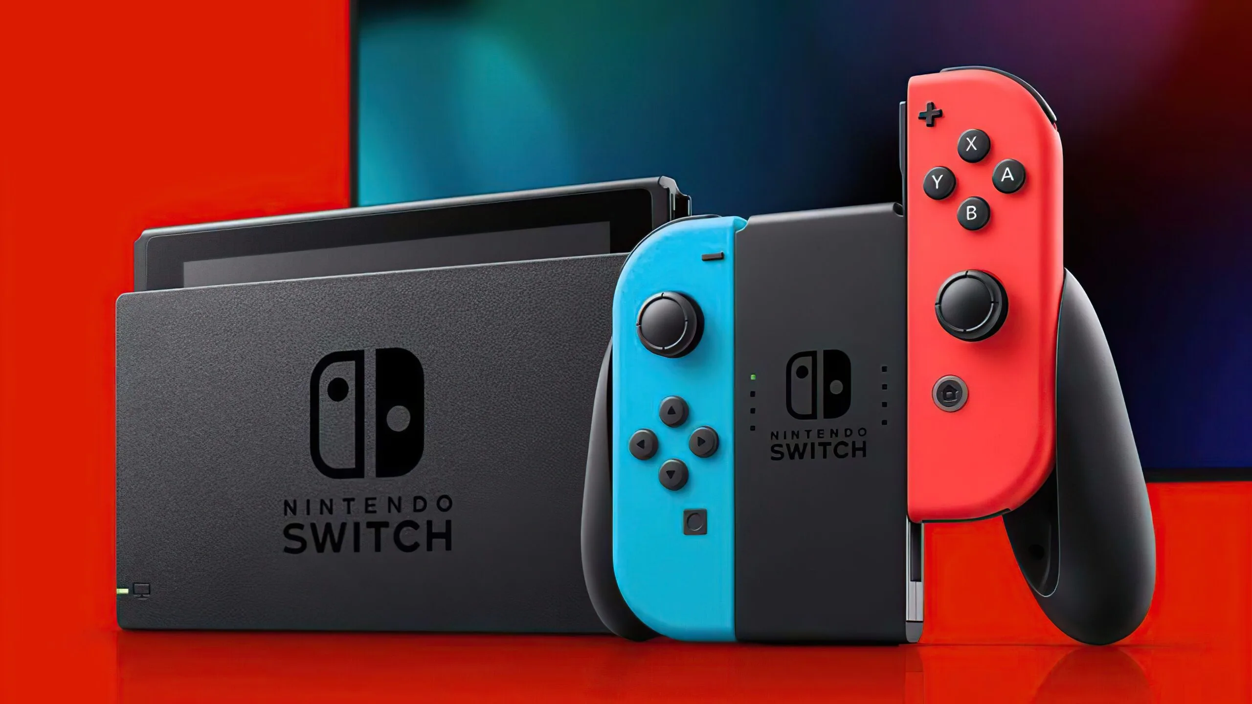
The Nintendo Switch 2 SOC may be produced on a 5nm process node and have a maximum clock speed of over 2.5 GHz, according to information unearthed today.
In a new video shared on YouTube, Doctre 81 detailed how, a few months back, they found the LinkedIn profile for a former Physical Design Engineer for Siliconist Technologies, who worked there from February 2020 to October 2022 on the T239 project for NVIDIA, which is said to be the Nintendo Switch 2 SOC.
Today, the YouTuber reported to have found another LinkedIn profile for another former Physical Design Engineer who worked at Siliconist Technologies during the same time as the other employee who actually put a more detailed summary of what they worked on during their time at the company, confirming it was an NVIDIA project without, however, mentioning any other specific. In this project summary, the former Siliconist Technologies employee mentions a 5nm process node and a maximum clock speed of 2.653 GHz, higher than the maximum clock speed of the original Nintendo Switch SOC, the TegraX1. As Nintendo is keeping a tight lid on its Nintendo Switch 2 console, however, we have to take what Doctre81 revealed in their video with a grain of salt.
Doesn't really matter, they don't need the switch to have bleeding edge performance, that isn't why it sells. It has to be affordable and using older processes helps achieve that.
No but it does need enough performance to be capable of running games in low quality modes. The Switch is so anemic that many big budget games are simply not even trying anymore as performant running can't be achieved without complete rewrites of engine code. So a better Switch that is at least a low spec gaming computer will enable more big games to many the effort of trying to support it.
Big time. Their chassis design will dictate performance too. They will get the best chip they can in a cost budget and then thermal/battery limits will dictate where that chip actually lies.
The steam deck is cool and a great device but the Switch 2 will be sleeker and nintendo won't settle for a 90min battery a whiney fan, and that has trade offs.
its meant for people in the tech space that can cross compare numbers with on the market devices. some basic specs give you a ball park estimation of what you kind of expect. Albeit, this is from WCCFTech, which theyll post just about any rumor, so take with huge grain of salt.
for laymans, ill do some of the cross comparison now.
5nm is the fabrication process used in AMDs current top end gpus, and current generation GPUs. In apple terms, same process used on its A14/A15 (iPhone 12-14) and M1/M2 (all current macbook devices) chips (only difference between the two generations is bleeding edge vs matured process, but they are effectively the same size).
For comparisons sake, the 5nm process is used by Nvidia's current generation RTX 4000 series gpus, but a special process for it (cusotmized basically for Nvidia). The clocks likely refer to CPU clocks so I will drop discussion of gpus here and move onto Nvidia's CPU offerings.
Nvidia essentially only puts CPUs on its enterprise and developer parts (the Tegra line, which is how the Switch ended up using it). Nvidias "Thor" would be the only device using 5nm, but little is known about Thor so I would refer to last gen Orin, which have development boards already on the market (in the same way the Tegra X1 in the switch also has Development boards on the market).
Orins Wikipedia section on pure numbers, the 2 middle SKUS, the 2 NX models are the ones that would likely go into a switch due to their TDP (10-25W), as 10W is the typical handheld TDP and 15-25 tends to be the TDP of devices when "Docked". Since last gen orin was capable of holding 2.2 Ghz CPU docked, then the switch SOC at least on paper, is closer to the full clocks when compared to the older Tegra X1 in the switch (which had it clocked to 1000 Ghz essentially, which is almost half of what the chip was designed for ~1800 which is seen in the commercially available Nvidia Shield TV). The CPU is a Arm Cortex A78, so I'd compare it to phones using it such as phones using the Snapdragon 888 cpu, but downclocked. Also forgot to put out there, Orins GPU is essentially similar to the Nvidia RTX 2050 mobile if you need some remote idea on how it would perform graphically.
Opinion post starts here:
Im on the boat who believes Nvidia is going to use Orin (or a varient of Orin just shrunk down to 5nm, as Orin is a 8nm product) as Nvidia does not like to do custom designs for any customer. It's the reason why Apple for instance, dropped nvidia and the last Nvidia GPU used in an apple product i believe was the GTX 670. The choice sounds like a very Nintendo thing to do, because 1. Nintendo has a history of choosing the lower end part nowadays and 2. Nintendo prefers to have their consoles sold at profit and not at a loss, so theyre more inclined to pick the cheaper device of any option. Given that Orin is an early covid design, it makes sense of the timeline as it would kinda be similar to the switch (the Switch launched in 2017, used the Tegra X1 which was in devices in 2015). Orin was produced early 2022, and the next Switch would likely launch in 2024
Smaller chips are a combination of faster and more power efficient than chips of a larger process size. The smaller the chips the less electrical impedance there is. That’s what makes processors hot. Less heat means less energy wasted and more potential to run the processor at a faster rate
basically it just means it's using newer chip-making processes to make the chip smaller and faster. It's sort of a no-brainer that a new chip would use some updated processes and likely run faster than one made 7 or 8 years ago.
Nothing until they actually announce something. Rumors aren't to be trusted at all, Nintendo has a history of disappointing on specs and making up for it with interesting gameplay.